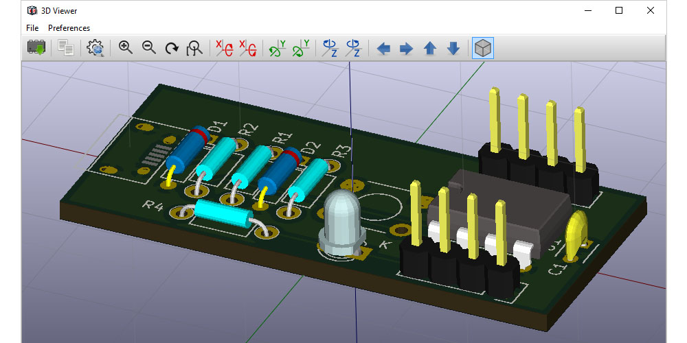
Printed circuit boards are found primarily on electronic devices. They have a significant role in facilitating the current flow between the components attached to the board. PCBs exist in various forms, and their design and manufacturing processes vary. During the production process, PCBs are constantly viewed in case any error or change arises. A unique tool called Kicad comes in handy in viewing the parts in 3D. Check out Kicad Gerber to learn more about the tool, its importance, and how to transfer the Gerber file after a design process to Kicad. Some PCB parts appear in all kinds, while others are customized to fit their application. We expound on the essential parts of a PCB below.
Essential Parts of a PCB
Printed circuit boards differ in several ways based on their uses. No particular number of components is right or wrong on a PCB as long as it functions correctly. The client influences the design, so some may have more components than others. However, there are common parts which include;
1. Layers
The layers or stack-ups allow you to distinguish between the different PCB types. There are those with single, double-sided, or multiple layers; single is the simplest while multiple is complex. The simple design of the single-layer PCBs is suitable for use in small objects and can be produced in bulk. In complex designs, a hole cutting through the layers facilitates routing; hence all components communicate, allowing the current flow. Different materials make the layers, each with a particular purpose on the board. Several factors influence the number of layers on PCBs, like the use, components, circuit size, and production cost.
2. Trace track
The track is primarily made of copper materials extracted from the PCB layer. However, manufacturers can use any material as long as it’s a good conductor of electricity. Traces enhance current flow to all components with minimal resistance, making it an essential part of PCB.
3. Solder Mask
Continuos current flow leads to the generation of heat. The solder mask insulates the PCB to protect each component from too much heat that may damage them. All conductive materials are separated from the copper pads, cutting off all contact to enhance the board’s safety.
4. Pad
This part is copper material located on two layers of the PCB is top and bottom. The pad gives room for soldering and mounting and provides mechanical support to all components on the PCB base.
5. Silkscreen Layer
It is also called the silk layer. It is found mainly on the PCB base, but the top layer can also have it if the client requests it. It helps mark all the components on the board, and the manufacturer can print any letter or image with ease due to the presence of the epoxy ink.
Bottom Line
Each part of a PCB has a major role to play to ensure it operates as desired. Before choosing a PCB design, determine which parts are standard and those that can be altered since various applications require different features. Seek advice from the electrical engineer to make the best choice for your PCB. Ensure each part is of good quality and performs well.

